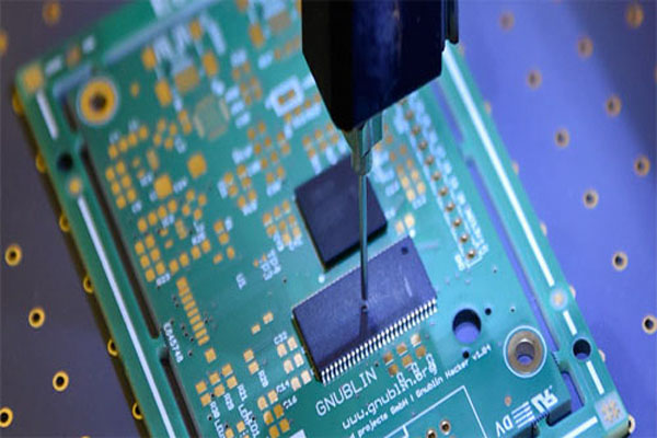
A printed circuit board (PCB) mechanically supports and electrically connects electronic components or electrical components using conductive tracks, pads and other features etched from one or more sheet layers of copper laminated onto and/or between sheet layers of a non-conductive substrate. Components are generally soldered onto the PCB to both electrically connect and mechanically fasten them to it.
Printed circuit boards are used in all but the simplest electronic products. They are also used in some electrical products, such as passive switch boxes.
Alternatives to PCBs include wire wrap and point-to-point construction, both once popular but now rarely used. PCBs require additional design effort to lay out the circuit, but manufacturing and assembly can be automated. Specialized CAD software is available to do much of the work of layout. Mass-producing circuits with PCBs is cheaper and faster than with other wiring methods, as components are mounted and wired in one operation. Large numbers of PCBs can be fabricated at the same time, and the layout only has to be done once. PCBs can also be made manually in small quantities, with reduced benefits.
© 2018 All rights reserved | OJASKAR SOLUTIONS INDIA PVT. LTD.
 011-28363017, 011-45061518, 7428709179